
 Commits $13B to Advanced HBM Packaging Facility in South Korea")
Key Highlights
- Memory chipmaker SK Hynix commits 19 trillion won (approximately $13 billion) to establish a new semiconductor packaging facility in South Korea.
- The facility, designated P&T7, will be situated in Heungdeok district within Cheongju and will specialize in cutting-edge chip packaging operations.
- Ground will be broken this month, with operations targeted for April 2026.
- Production focus centers on high-bandwidth memory (HBM) technology, essential components for artificial intelligence data centres and Nvidia’s processor ecosystem.
- The company has already initiated volume manufacturing of advanced memory solutions for Nvidia’s forthcoming Vera Rubin AI processor platform.
South Korean memory giant SK Hynix revealed plans Wednesday to allocate approximately 19 trillion won — equivalent to roughly $13 billion — toward constructing a state-of-the-art packaging fabrication facility on home soil. The installation, which carries the designation P&T7, will occupy a site within Cheongju’s Heungdeok district.
Ground-breaking activities are scheduled to commence this month, the company disclosed through a regulatory submission. This capital deployment represents among the most substantial single-site investments the semiconductor manufacturer has undertaken in its corporate history.
The new manufacturing hub will concentrate entirely on sophisticated packaging techniques — specialized processes required to construct high-bandwidth memory (HBM) components. This particular memory architecture underpins the vast majority of contemporary AI acceleration hardware, notably products manufactured by Nvidia.
As a leading global memory semiconductor producer and crucial Nvidia supply partner, SK Hynix has witnessed explosive demand growth driven by worldwide AI infrastructure expansion.
The Strategic Importance of Sophisticated Packaging
Sophisticated packaging transcends simple assembly operations — it fundamentally dictates data transfer velocity and operational efficiency within memory components. For artificial intelligence computing tasks, these performance characteristics prove absolutely vital.
HBM technology employs vertically stacked memory layers interconnected via microscopic vertical pathways. Achieving manufacturing precision and consistency at commercial volumes demands both exceptional technical expertise and substantial capital resources.
Company representatives indicated they have been accelerating capacity expansion timelines to accommodate surging order volumes. During the first months of this year, the firm fast-tracked the launch of an additional memory chip production facility in South Korea for identical strategic reasons.
The disclosed investment amount remains flexible and may be adjusted according to evolving market dynamics and corporate strategic considerations, SK Hynix clarified in its regulatory documentation.
Vera Rubin Memory Modules Enter Mass Production Phase
Earlier in the week, SK Hynix announced it had commenced volume manufacturing of an advanced-generation memory solution engineered explicitly for Nvidia’s Vera Rubin AI processor — representing Nvidia’s successor platform following Blackwell.
This production milestone emerged mere days ahead of the $13 billion facility disclosure, emphasizing the accelerated pace at which the corporation is advancing to cement its supply chain positioning.
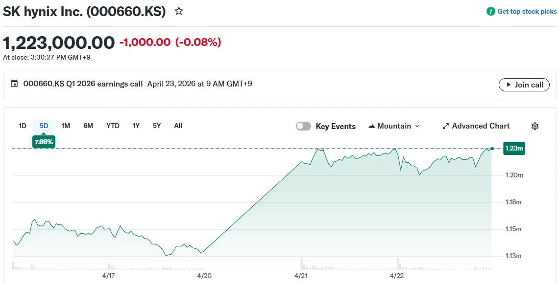
Shares declined approximately 1% Wednesday following the investment revelation. This modest retreat followed the stock’s climb to unprecedented highs during the previous trading session.
As of Wednesday’s close, SK Hynix maintains its listing on the Korea Exchange under ticker symbol 000660. The corporation has not yet published a projected timeline for P&T7 facility completion.